What is Printed Circuit Board Assembly (PCBA)?
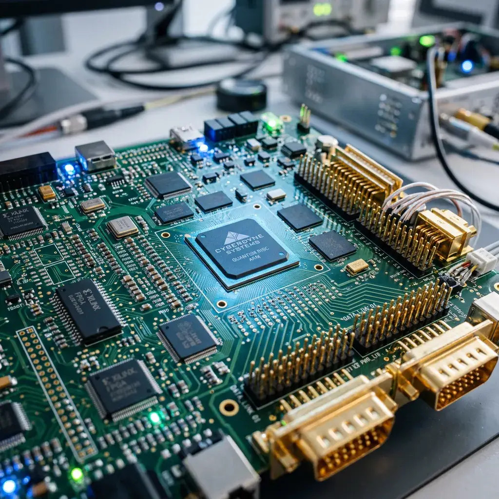
Printed circuit board assembly (PCBA) is the process of soldering or assembling electronic components onto a bare printed circuit board (PCB) to create a functional electronic circuit. The bare PCB — with its copper traces, pads, and vias — serves as both the mechanical foundation and electrical interconnection layer for the components mounted on it.
PCBA is the core competency of any Electronic Manufacturing Services (EMS) provider. The quality of printed circuit board assembly directly determines the reliability, performance, and lifecycle of the final electronic product.
The Complete PCBA Process
Step 1: Solder Paste Printing
The assembly process begins with applying solder paste to the PCB through a precision stencil. The stencil apertures align exactly with the surface mount pads, depositing precise volumes of solder paste. Solder Paste Inspection (SPI) machines verify correct paste volume and alignment before proceeding.
Step 2: SMT Component Placement
High-speed SMT pick-and-place machines mount surface mount components onto the solder paste deposits. Modern machines handle components as small as 0201 (0.25mm × 0.125mm) and as complex as fine-pitch BGAs with hundreds of solder balls.
Step 3: Reflow Soldering
Reflow soldering permanently bonds the SMT components to the printed circuit board. The board passes through a convection oven with precisely controlled temperature zones, melting the solder paste and forming reliable metallurgical bonds.
Step 4: Through Hole Component Insertion
For mixed-technology boards, through hole components are inserted after SMT reflow. This includes connectors, transformers, large capacitors, and other components requiring mechanical strength.
Step 5: Wave or Selective Soldering
Through hole components are soldered using wave soldering or selective soldering processes. Selective soldering is preferred for boards with dense SMT components on the solder side.
Step 6: Inspection (AOI & X-Ray)
Automated Optical Inspection (AOI) examines every solder joint for defects including bridges, insufficient solder, tombstoning, and component misalignment. X-ray inspection verifies hidden solder joints under BGAs and QFN packages.
Step 7: In-Circuit Testing (ICT)
In-circuit testing verifies the electrical integrity of every board by probing test points and measuring component values, shorts, and opens.
Step 8: Functional Testing
Final functional testing verifies the assembled board performs correctly under real operating conditions, including firmware uploading and application-specific tests.
Step 9: Conformal Coating (When Required)
For applications in harsh environments, conformal coating or epoxy filling protects the finished assembly from moisture, chemicals, and contaminants.
Quality Standards in PCBA
- IPC-A-610: Acceptability of Electronic Assemblies — the worldwide benchmark
- IPC J-STD-001: Soldering standards for electronic assemblies
- ISO 9001: Quality management system
- RoHS: Restriction of hazardous substances in electronics
PCBA at TOS Lanka
TOS Lanka delivers comprehensive printed circuit board assembly services with:
- State-of-the-art SMT lines with Panasonic high-speed placement
- Full THT capability with wave and manual soldering
- Advanced testing and inspection at every stage
- Rapid prototyping through to volume production
- Complete box build integration
Contact TOS Lanka to discuss your printed circuit board assembly requirements.